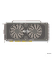
AMD Radeon PRO WX 3100 AMD Radeon PRO WX 3100
XFX Radeon Pro Duo XFX Radeon Pro Duo
VS

Comparision AMD Radeon PRO WX 3100 vs XFX Radeon Pro Duo

AMD Radeon PRO WX 3100

WINNER
AMD Radeon PRO WX 3100

Rating: 9 points
XFX Radeon Pro Duo

XFX Radeon Pro Duo

Rating: 0 points
Grade
AMD Radeon PRO WX 3100
XFX Radeon Pro Duo
Performance
5
5
Memory
3
3
General information
7
0
Functions
7
7
Benchmark tests
1
0
Ports
0
3

Top specs and features

Passmark score

AMD Radeon PRO WX 3100: 2671 XFX Radeon Pro Duo:

3DMark Cloud Gate GPU benchmark score

AMD Radeon PRO WX 3100: 18624 XFX Radeon Pro Duo:

3DMark Fire Strike Score

AMD Radeon PRO WX 3100: 2494 XFX Radeon Pro Duo:

3DMark Fire Strike Graphics test score

AMD Radeon PRO WX 3100: 2686 XFX Radeon Pro Duo:

3DMark 11 Performance GPU benchmark score

AMD Radeon PRO WX 3100: 3711 XFX Radeon Pro Duo:

Description

The AMD Radeon PRO WX 3100 video card is based on the GCN 4.0 architecture. XFX Radeon Pro Duo on the GCN 3.0 architecture. The first has 2200 million transistors. The second is 8900 million. AMD Radeon PRO WX 3100 has a transistor size of 14 nm versus 28.

The base clock speed of the first video card is 925 MHz versus 1000 MHz for the second.

Let's move on to memory. AMD Radeon PRO WX 3100 has 4 GB. XFX Radeon Pro Duo has 4 GB installed. The bandwidth of the first video card is 96 Gb/s versus 1024 Gb/s of the second.

FLOPS of AMD Radeon PRO WX 3100 is 1.21. At XFX Radeon Pro Duo 16.17.

Goes to tests in benchmarks. In the Passmark benchmark, AMD Radeon PRO WX 3100 scored 2671 points. And here is the second card There is no data points. In 3DMark, the first model scored 2686 points. Second There is no data points.

In terms of interfaces. The first video card is connected using PCIe 3.0 x8. The second is There is no data. Video card AMD Radeon PRO WX 3100 has Directx version 12. Video card XFX Radeon Pro Duo -- Directx version - 12.

Regarding cooling, AMD Radeon PRO WX 3100 has 65W heat dissipation requirements versus 350W for XFX Radeon Pro Duo.

Why AMD Radeon PRO WX 3100 is better than XFX Radeon Pro Duo

  • Effective memory speed 6000 MHz против 1000 MHz, more on 500%
  • Gpu memory speed 1500 MHz против 500 MHz, more on 200%
  • Power Consumption (TDP) 65 W против 350 W, less by -81%
  • Technological process 14 nm против 28 nm, less by -50%

AMD Radeon PRO WX 3100 vs XFX Radeon Pro Duo: highlights

AMD Radeon PRO WX 3100
XFX Radeon Pro Duo
XFX Radeon Pro Duo
Performance
GPU base clock speed
The graphics processing unit (GPU) has a high clock speed.
925 MHz
max 2457
Average: 1124.9 MHz
1000 MHz
max 2457
Average: 1124.9 MHz
Gpu memory speed
This is an important aspect for calculating memory bandwidth.
1500 MHz
max 16000
Average: 1468 MHz
500 MHz
max 16000
Average: 1468 MHz
FLOPS
Measuring the processing power of a processor is called FLOPS.
1.21 TFLOPS
max 1142.32
Average: 53 TFLOPS
16.17 TFLOPS
max 1142.32
Average: 53 TFLOPS
RAM
RAM in video cards (also known as video memory or VRAM) is a special type of memory used by a video card to store graphics data. It serves as a temporary buffer for textures, shaders, geometry, and other graphics resources that are needed to display images on the screen. More RAM allows the graphics card to work with more data and handle more complex graphic scenes with high resolution and detail. Show more
4 GB
max 128
Average: 4.6 GB
8 GB
max 128
Average: 4.6 GB
Number of PCIe lanes
The number of PCIe lanes in video cards determines the speed and bandwidth of data transfer between the video card and other computer components through the PCIe interface. The more PCIe lanes a video card has, the more bandwidth and ability to communicate with other computer components. Show more
8
max 16
Average:
max 16
Average:
Pixel rendering speed
The higher the pixel rendering speed, the smoother and more realistic the display of graphics and the movement of objects on the screen will be.
20 GTexel/s    
max 563
Average: 94.3 GTexel/s    
128 GTexel/s    
max 563
Average: 94.3 GTexel/s    
TMUs
Responsible for texturing objects in 3D graphics. TMU provides textures to the surfaces of objects, which gives them a realistic look and detail. The number of TMUs in a video card determines its ability to process textures. The more TMUs, the more textures can be processed at the same time, which contributes to better texturing of objects and increases the realism of graphics. Show more
32
max 880
Average: 140.1
max 880
Average: 140.1
ROPs
Responsible for the final processing of pixels and their display on the screen. ROPs perform various operations on pixels, such as blending colors, applying transparency, and writing to the framebuffer. The number of ROPs in a video card affects its ability to process and display graphics. The more ROPs, the more pixels and image fragments can be processed and displayed on the screen at the same time. A higher number of ROPs generally results in faster and more efficient graphics rendering and better performance in games and graphics applications. Show more
16
max 256
Average: 56.8
128
max 256
Average: 56.8
Number of shader blocks
The number of shader units in video cards refers to the number of parallel processors that perform computational operations in the GPU. The more shader units in the video card, the more computing resources are available for processing graphics tasks. Show more
512
max 17408
Average:
8192
max 17408
Average:
Processor cores
The number of processor cores in a video card indicates the number of independent computing units capable of performing tasks in parallel. More cores allow for more efficient load balancing and processing of more graphics data, leading to improved performance and rendering quality. Show more
8
max 220
Average:
max 220
Average:
L2 cache size
Used to temporarily store data and instructions used by the graphics card when performing graphics calculations. A larger L2 cache allows the graphics card to store more data and instructions, which helps speed up the processing of graphics operations. Show more
512
There is no data
Turbo gpu
If the GPU speed has dropped below its limit, then to improve performance, it can go to a high clock speed.
1219 MHz
max 2903
Average: 1514 MHz
MHz
max 2903
Average: 1514 MHz
Texture size
A certain number of textured pixels are displayed on the screen every second.
39.01 GTexels/s
max 756.8
Average: 145.4 GTexels/s
512 GTexels/s
max 756.8
Average: 145.4 GTexels/s
architecture name
GCN 4.0
GCN 3.0
GPU name
Lexa
Capsaicin
Memory
Memory bandwidth
This is the rate at which the device stores or reads information.
96 GB/s
max 2656
Average: 257.8 GB/s
1024 GB/s
max 2656
Average: 257.8 GB/s
Effective memory speed
The effective memory clock is calculated from the size and transfer rate of the memory information. The performance of the device in applications depends on the clock frequency. The higher it is, the better. Show more
6000 MHz
max 19500
Average: 6984.5 MHz
1000 MHz
max 19500
Average: 6984.5 MHz
RAM
RAM in video cards (also known as video memory or VRAM) is a special type of memory used by a video card to store graphics data. It serves as a temporary buffer for textures, shaders, geometry, and other graphics resources that are needed to display images on the screen. More RAM allows the graphics card to work with more data and handle more complex graphic scenes with high resolution and detail. Show more
4 GB
max 128
Average: 4.6 GB
8 GB
max 128
Average: 4.6 GB
GDDR memory versions
Latest versions of GDDR memory provide high data transfer rates to improve overall performance
5
max 6
Average: 4.9
max 6
Average: 4.9
Memory bus width
A wide memory bus means that it can transfer more information in one cycle. This property affects memory performance as well as the overall performance of the device's graphics card. Show more
128 bit
max 8192
Average: 283.9 bit
4096 bit
max 8192
Average: 283.9 bit
General information
Crystal size
The physical dimensions of the chip on which the transistors, microcircuits and other components necessary for the operation of the video card are located. The larger the die size, the more space the GPU takes up on the graphics card. Larger die sizes can provide more computing resources such as CUDA cores or tensor cores, which can result in increased performance and graphics processing capabilities. Show more
103
max 826
Average: 356.7
max 826
Average: 356.7
Length
170
max 524
Average: 250.2
max 524
Average: 250.2
Generation
A new generation of graphics card usually includes improved architecture, higher performance, more efficient use of power, improved graphics capabilities, and new features. Show more
Radeon Pro
There is no data
Manufacturer
GlobalFoundries
There is no data
Power supply power
When choosing a power supply for a video card, you must take into account the power requirements of the video card manufacturer, as well as other computer components. Show more
250
max 1300
Average:
max 1300
Average:
Year of issue
2017
max 2023
Average:
max 2023
Average:
Power Consumption (TDP)
Heat Dissipation Requirements (TDP) is the maximum possible amount of energy dissipated by the cooling system. The lower the TDP, the less power will be consumed Show more
65 W
Average: 160 W
350 W
Average: 160 W
Technological process
The small size of the semiconductors means this is a new generation chip.
14 nm
Average: 34.7 nm
28 nm
Average: 34.7 nm
Number of transistors
The higher their number, the more processor power this indicates.
2200 million
max 80000
Average: 7150 million
8900 million
max 80000
Average: 7150 million
PCIe connection interface
A considerable speed of the expansion card used to connect the computer to the peripherals is provided. The updated versions offer impressive bandwidth and high performance. Show more
3
max 4
Average: 3
3
max 4
Average: 3
Width
67 mm
max 421.7
Average: 192.1 mm
281 mm
max 421.7
Average: 192.1 mm
Purpose
Mobile Workstations
There is no data
Price at the time of release
199 $
max 419999
Average: 5679.5 $
$
max 419999
Average: 5679.5 $
Functions
OpenGL Version
OpenGL provides access to the graphics card's hardware capabilities for displaying 2D and 3D graphics objects. New versions of OpenGL may include support for new graphical effects, performance optimizations, bug fixes, and other improvements. Show more
4.6
max 4.6
Average:
4.5
max 4.6
Average:
DirectX
Used in demanding games, providing improved graphics
12
max 12.2
Average: 11.4
12
max 12.2
Average: 11.4
Shader model version
The higher the version of the shader model in the video card, the more functions and possibilities are available for programming graphic effects.
6.4
max 6.7
Average: 5.9
max 6.7
Average: 5.9
Benchmark tests
Passmark score
The Passmark Video Card Test is a program for measuring and comparing the performance of a graphics system. It conducts various tests and calculations to evaluate the speed and performance of a graphics card in various areas. Show more
2671
max 30117
Average: 7628.6
max 30117
Average: 7628.6
3DMark Cloud Gate GPU benchmark score
18624
max 196940
Average: 80042.3
max 196940
Average: 80042.3
3DMark Fire Strike Score
2494
max 39424
Average: 12463
max 39424
Average: 12463
3DMark Fire Strike Graphics test score
It measures and compares the ability of a graphics card to handle high-resolution 3D graphics with various graphical effects. The Fire Strike Graphics test includes complex scenes, lighting, shadows, particles, reflections, and other graphical effects to evaluate the graphics card's performance in gaming and other demanding graphics scenarios. Show more
2686
max 51062
Average: 11859.1
max 51062
Average: 11859.1
3DMark 11 Performance GPU benchmark score
3711
max 59675
Average: 18799.9
max 59675
Average: 18799.9
3DMark Vantage Performance test score
11766
max 97329
Average: 37830.6
max 97329
Average: 37830.6
3DMark Ice Storm GPU benchmark score
177324
max 539757
Average: 372425.7
max 539757
Average: 372425.7
SPECviewperf 12 test score - Solidworks
29
max 203
Average: 62.4
max 203
Average: 62.4
SPECviewperf 12 test score - specvp12 sw-03
The sw-03 test includes visualization and modeling of objects using various graphic effects and techniques such as shadows, lighting, reflections and others. Show more
29
max 203
Average: 64
max 203
Average: 64
SPECviewperf 12 test evaluation - Siemens NX
17
max 213
Average: 14
max 213
Average: 14
SPECviewperf 12 test score - specvp12 showcase-01
The showcase-01 test is a scene with complex 3D models and effects that demonstrates the capabilities of the graphics system in processing complex scenes. Show more
6
max 239
Average: 121.3
max 239
Average: 121.3
SPECviewperf 12 test score - Showcase
6
max 180
Average: 108.4
max 180
Average: 108.4
SPECviewperf 12 test score - Medical
4
max 107
Average: 39.6
max 107
Average: 39.6
SPECviewperf 12 test score - specvp12 mediacal-01
4
max 107
Average: 39
max 107
Average: 39
SPECviewperf 12 test score - Maya
11
max 182
Average: 129.8
max 182
Average: 129.8
SPECviewperf 12 test score - specvp12 maya-04
11
max 185
Average: 132.8
max 185
Average: 132.8
SPECviewperf 12 Test Evaluation - Creo
18
max 154
Average: 49.5
max 154
Average: 49.5
SPECviewperf 12 test score - specvp12 creo-01
18
max 154
Average: 52.5
max 154
Average: 52.5
SPECviewperf 12 test score - specvp12 catia-04
16
max 190
Average: 91.5
max 190
Average: 91.5
SPECviewperf 12 test score - Catia
16
max 190
Average: 88.6
max 190
Average: 88.6
Ports
mini-DisplayPort
Allows you to connect to a display using mini DisplayPort
2
max 8
Average: 2.1
max 8
Average: 2.1
Interface
PCIe 3.0 x8
There is no data

FAQ

How does the AMD Radeon PRO WX 3100 processor perform in benchmarks?

Passmark AMD Radeon PRO WX 3100 scored 2671 points. The second video card scored There is no data points in Passmark.

What FLOPS do video cards have?

FLOPS AMD Radeon PRO WX 3100 is 1.21 TFLOPS. But the second video card has FLOPS equal to 16.17 TFLOPS.

What power consumption?

AMD Radeon PRO WX 3100 65 Watt. XFX Radeon Pro Duo 350 Watt.

How fast are AMD Radeon PRO WX 3100 and XFX Radeon Pro Duo?

AMD Radeon PRO WX 3100 operates at 925 MHz. In this case, the maximum frequency reaches 1219 MHz. The clock base frequency of XFX Radeon Pro Duo reaches 1000 MHz. In turbo mode it reaches There is no data MHz.

What kind of memory do graphics cards have?

AMD Radeon PRO WX 3100 supports GDDR5. Installed 4 GB of RAM. Throughput reaches 96 GB/s. XFX Radeon Pro Duo works with GDDRThere is no data. The second one has 8 GB of RAM installed. Its bandwidth is 96 GB/s.

How many HDMI connectors do they have?

AMD Radeon PRO WX 3100 has There is no data HDMI outputs. XFX Radeon Pro Duo is equipped with 1 HDMI outputs.

What power connectors are used?

AMD Radeon PRO WX 3100 uses There is no data. XFX Radeon Pro Duo is equipped with There is no data HDMI outputs.

What architecture are video cards based on?

AMD Radeon PRO WX 3100 is built on GCN 4.0. XFX Radeon Pro Duo uses the GCN 3.0 architecture.

What graphics processor is being used?

AMD Radeon PRO WX 3100 is equipped with Lexa. XFX Radeon Pro Duo is set to Capsaicin.

How many PCIe lanes

The first graphics card has 8 PCIe lanes. And the PCIe version is 3. XFX Radeon Pro Duo 8 PCIe lanes. PCIe version 3.

How many transistors?

AMD Radeon PRO WX 3100 has 2200 million transistors. XFX Radeon Pro Duo has 8900 million transistors