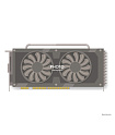
NVIDIA GeForce RTX 2070 Super NVIDIA GeForce RTX 2070 Super
AMD Radeon PRO WX 3100 AMD Radeon PRO WX 3100
VS

Comparision NVIDIA GeForce RTX 2070 Super vs AMD Radeon PRO WX 3100

NVIDIA GeForce RTX 2070 Super

WINNER
NVIDIA GeForce RTX 2070 Super

Rating: 58 points
AMD Radeon PRO WX 3100

AMD Radeon PRO WX 3100

Rating: 9 points
Grade
NVIDIA GeForce RTX 2070 Super
AMD Radeon PRO WX 3100
Performance
7
5
Memory
6
3
General information
7
7
Functions
9
7
Benchmark tests
6
1
Ports
10
0

Top specs and features

Passmark score

NVIDIA GeForce RTX 2070 Super: 17266 AMD Radeon PRO WX 3100: 2671

3DMark Cloud Gate GPU benchmark score

NVIDIA GeForce RTX 2070 Super: 122452 AMD Radeon PRO WX 3100: 18624

3DMark Fire Strike Score

NVIDIA GeForce RTX 2070 Super: 20406 AMD Radeon PRO WX 3100: 2494

3DMark Fire Strike Graphics test score

NVIDIA GeForce RTX 2070 Super: 23263 AMD Radeon PRO WX 3100: 2686

3DMark 11 Performance GPU benchmark score

NVIDIA GeForce RTX 2070 Super: 31997 AMD Radeon PRO WX 3100: 3711

Description

The NVIDIA GeForce RTX 2070 Super video card is based on the Turing architecture. AMD Radeon PRO WX 3100 on the GCN 4.0 architecture. The first has 13600 million transistors. The second is 2200 million. NVIDIA GeForce RTX 2070 Super has a transistor size of 12 nm versus 14.

The base clock speed of the first video card is 1605 MHz versus 925 MHz for the second.

Let's move on to memory. NVIDIA GeForce RTX 2070 Super has 8 GB. AMD Radeon PRO WX 3100 has 8 GB installed. The bandwidth of the first video card is 448 Gb/s versus 96 Gb/s of the second.

FLOPS of NVIDIA GeForce RTX 2070 Super is 9.28. At AMD Radeon PRO WX 3100 1.21.

Goes to tests in benchmarks. In the Passmark benchmark, NVIDIA GeForce RTX 2070 Super scored 17266 points. And here is the second card 2671 points. In 3DMark, the first model scored 23263 points. Second 2686 points.

In terms of interfaces. The first video card is connected using PCIe 3.0 x16. The second is PCIe 3.0 x8. Video card NVIDIA GeForce RTX 2070 Super has Directx version 12.2. Video card AMD Radeon PRO WX 3100 -- Directx version - 12.

Regarding cooling, NVIDIA GeForce RTX 2070 Super has 215W heat dissipation requirements versus 65W for AMD Radeon PRO WX 3100.

Why NVIDIA GeForce RTX 2070 Super is better than AMD Radeon PRO WX 3100

  • Passmark score 17266 против 2671 , more on 546%
  • 3DMark Cloud Gate GPU benchmark score 122452 против 18624 , more on 557%
  • 3DMark Fire Strike Score 20406 против 2494 , more on 718%
  • 3DMark Fire Strike Graphics test score 23263 против 2686 , more on 766%
  • 3DMark 11 Performance GPU benchmark score 31997 против 3711 , more on 762%
  • 3DMark Vantage Performance test score 65706 против 11766 , more on 458%
  • 3DMark Ice Storm GPU benchmark score 478763 против 177324 , more on 170%
  • GPU base clock speed 1605 MHz против 925 MHz, more on 74%

NVIDIA GeForce RTX 2070 Super vs AMD Radeon PRO WX 3100: highlights

NVIDIA GeForce RTX 2070 Super
AMD Radeon PRO WX 3100
Performance
GPU base clock speed
The graphics processing unit (GPU) has a high clock speed.
1605 MHz
max 2457
Average: 1124.9 MHz
925 MHz
max 2457
Average: 1124.9 MHz
Gpu memory speed
This is an important aspect for calculating memory bandwidth.
1750 MHz
max 16000
Average: 1468 MHz
1500 MHz
max 16000
Average: 1468 MHz
FLOPS
Measuring the processing power of a processor is called FLOPS.
9.28 TFLOPS
max 1142.32
Average: 53 TFLOPS
1.21 TFLOPS
max 1142.32
Average: 53 TFLOPS
RAM
RAM in video cards (also known as video memory or VRAM) is a special type of memory used by a video card to store graphics data. It serves as a temporary buffer for textures, shaders, geometry, and other graphics resources that are needed to display images on the screen. More RAM allows the graphics card to work with more data and handle more complex graphic scenes with high resolution and detail. Show more
8 GB
max 128
Average: 4.6 GB
4 GB
max 128
Average: 4.6 GB
Number of PCIe lanes
The number of PCIe lanes in video cards determines the speed and bandwidth of data transfer between the video card and other computer components through the PCIe interface. The more PCIe lanes a video card has, the more bandwidth and ability to communicate with other computer components. Show more
16
max 16
Average:
8
max 16
Average:
L1 cache size
The amount of L1 cache in video cards is usually small and is measured in kilobytes (KB) or megabytes (MB). It is designed to temporarily store the most active and frequently used data and instructions, allowing the graphics card to access them faster and reduce delays in graphics operations. Show more
64
There is no data
Pixel rendering speed
The higher the pixel rendering speed, the smoother and more realistic the display of graphics and the movement of objects on the screen will be.
113 GTexel/s    
max 563
Average: 94.3 GTexel/s    
20 GTexel/s    
max 563
Average: 94.3 GTexel/s    
TMUs
Responsible for texturing objects in 3D graphics. TMU provides textures to the surfaces of objects, which gives them a realistic look and detail. The number of TMUs in a video card determines its ability to process textures. The more TMUs, the more textures can be processed at the same time, which contributes to better texturing of objects and increases the realism of graphics. Show more
160
max 880
Average: 140.1
32
max 880
Average: 140.1
ROPs
Responsible for the final processing of pixels and their display on the screen. ROPs perform various operations on pixels, such as blending colors, applying transparency, and writing to the framebuffer. The number of ROPs in a video card affects its ability to process and display graphics. The more ROPs, the more pixels and image fragments can be processed and displayed on the screen at the same time. A higher number of ROPs generally results in faster and more efficient graphics rendering and better performance in games and graphics applications. Show more
64
max 256
Average: 56.8
16
max 256
Average: 56.8
Number of shader blocks
The number of shader units in video cards refers to the number of parallel processors that perform computational operations in the GPU. The more shader units in the video card, the more computing resources are available for processing graphics tasks. Show more
2560
max 17408
Average:
512
max 17408
Average:
L2 cache size
Used to temporarily store data and instructions used by the graphics card when performing graphics calculations. A larger L2 cache allows the graphics card to store more data and instructions, which helps speed up the processing of graphics operations. Show more
4000
512
Turbo gpu
If the GPU speed has dropped below its limit, then to improve performance, it can go to a high clock speed.
1770 MHz
max 2903
Average: 1514 MHz
1219 MHz
max 2903
Average: 1514 MHz
Texture size
A certain number of textured pixels are displayed on the screen every second.
283.2 GTexels/s
max 756.8
Average: 145.4 GTexels/s
39.01 GTexels/s
max 756.8
Average: 145.4 GTexels/s
architecture name
Turing
GCN 4.0
GPU name
TU104
Lexa
Memory
Memory bandwidth
This is the rate at which the device stores or reads information.
448 GB/s
max 2656
Average: 257.8 GB/s
96 GB/s
max 2656
Average: 257.8 GB/s
Effective memory speed
The effective memory clock is calculated from the size and transfer rate of the memory information. The performance of the device in applications depends on the clock frequency. The higher it is, the better. Show more
14000 MHz
max 19500
Average: 6984.5 MHz
6000 MHz
max 19500
Average: 6984.5 MHz
RAM
RAM in video cards (also known as video memory or VRAM) is a special type of memory used by a video card to store graphics data. It serves as a temporary buffer for textures, shaders, geometry, and other graphics resources that are needed to display images on the screen. More RAM allows the graphics card to work with more data and handle more complex graphic scenes with high resolution and detail. Show more
8 GB
max 128
Average: 4.6 GB
4 GB
max 128
Average: 4.6 GB
GDDR memory versions
Latest versions of GDDR memory provide high data transfer rates to improve overall performance
6
max 6
Average: 4.9
5
max 6
Average: 4.9
Memory bus width
A wide memory bus means that it can transfer more information in one cycle. This property affects memory performance as well as the overall performance of the device's graphics card. Show more
256 bit
max 8192
Average: 283.9 bit
128 bit
max 8192
Average: 283.9 bit
General information
Crystal size
The physical dimensions of the chip on which the transistors, microcircuits and other components necessary for the operation of the video card are located. The larger the die size, the more space the GPU takes up on the graphics card. Larger die sizes can provide more computing resources such as CUDA cores or tensor cores, which can result in increased performance and graphics processing capabilities. Show more
545
max 826
Average: 356.7
103
max 826
Average: 356.7
Length
268
max 524
Average: 250.2
170
max 524
Average: 250.2
Generation
A new generation of graphics card usually includes improved architecture, higher performance, more efficient use of power, improved graphics capabilities, and new features. Show more
GeForce 20
Radeon Pro
Manufacturer
TSMC
GlobalFoundries
Power supply power
When choosing a power supply for a video card, you must take into account the power requirements of the video card manufacturer, as well as other computer components. Show more
550
max 1300
Average:
250
max 1300
Average:
Year of issue
2019
max 2023
Average:
2017
max 2023
Average:
Power Consumption (TDP)
Heat Dissipation Requirements (TDP) is the maximum possible amount of energy dissipated by the cooling system. The lower the TDP, the less power will be consumed Show more
215 W
Average: 160 W
65 W
Average: 160 W
Technological process
The small size of the semiconductors means this is a new generation chip.
12 nm
Average: 34.7 nm
14 nm
Average: 34.7 nm
Number of transistors
The higher their number, the more processor power this indicates.
13600 million
max 80000
Average: 7150 million
2200 million
max 80000
Average: 7150 million
PCIe connection interface
A considerable speed of the expansion card used to connect the computer to the peripherals is provided. The updated versions offer impressive bandwidth and high performance. Show more
3
max 4
Average: 3
3
max 4
Average: 3
Width
117 mm
max 421.7
Average: 192.1 mm
67 mm
max 421.7
Average: 192.1 mm
Height
34 mm
max 620
Average: 89.6 mm
mm
max 620
Average: 89.6 mm
Purpose
Desktop
Mobile Workstations
Price at the time of release
499 $
max 419999
Average: 5679.5 $
199 $
max 419999
Average: 5679.5 $
Functions
OpenGL Version
OpenGL provides access to the graphics card's hardware capabilities for displaying 2D and 3D graphics objects. New versions of OpenGL may include support for new graphical effects, performance optimizations, bug fixes, and other improvements. Show more
4.6
max 4.6
Average:
4.6
max 4.6
Average:
DirectX
Used in demanding games, providing improved graphics
12.2
max 12.2
Average: 11.4
12
max 12.2
Average: 11.4
Shader model version
The higher the version of the shader model in the video card, the more functions and possibilities are available for programming graphic effects.
6.6
max 6.7
Average: 5.9
6.4
max 6.7
Average: 5.9
Vulkan version
A higher version of Vulkan usually means a larger set of features, optimizations, and enhancements that software developers can use to create better and more realistic graphical applications and games. Show more
1.3
max 1.3
Average:
max 1.3
Average:
CUDA Version
Allows you to use the compute cores of your graphics card to perform parallel computing, which can be useful in areas such as scientific research, deep learning, image processing, and other computationally intensive tasks. Show more
7.5
max 9
Average:
max 9
Average:
Benchmark tests
Passmark score
The Passmark Video Card Test is a program for measuring and comparing the performance of a graphics system. It conducts various tests and calculations to evaluate the speed and performance of a graphics card in various areas. Show more
17266
max 30117
Average: 7628.6
2671
max 30117
Average: 7628.6
3DMark Cloud Gate GPU benchmark score
122452
max 196940
Average: 80042.3
18624
max 196940
Average: 80042.3
3DMark Fire Strike Score
20406
max 39424
Average: 12463
2494
max 39424
Average: 12463
3DMark Fire Strike Graphics test score
It measures and compares the ability of a graphics card to handle high-resolution 3D graphics with various graphical effects. The Fire Strike Graphics test includes complex scenes, lighting, shadows, particles, reflections, and other graphical effects to evaluate the graphics card's performance in gaming and other demanding graphics scenarios. Show more
23263
max 51062
Average: 11859.1
2686
max 51062
Average: 11859.1
3DMark 11 Performance GPU benchmark score
31997
max 59675
Average: 18799.9
3711
max 59675
Average: 18799.9
3DMark Vantage Performance test score
65706
max 97329
Average: 37830.6
11766
max 97329
Average: 37830.6
3DMark Ice Storm GPU benchmark score
478763
max 539757
Average: 372425.7
177324
max 539757
Average: 372425.7
SPECviewperf 12 test score - Solidworks
69
max 203
Average: 62.4
29
max 203
Average: 62.4
SPECviewperf 12 test score - specvp12 sw-03
The sw-03 test includes visualization and modeling of objects using various graphic effects and techniques such as shadows, lighting, reflections and others. Show more
67
max 203
Average: 64
29
max 203
Average: 64
SPECviewperf 12 test evaluation - Siemens NX
12
max 213
Average: 14
17
max 213
Average: 14
SPECviewperf 12 test score - specvp12 showcase-01
The showcase-01 test is a scene with complex 3D models and effects that demonstrates the capabilities of the graphics system in processing complex scenes. Show more
120
max 239
Average: 121.3
6
max 239
Average: 121.3
SPECviewperf 12 test score - Showcase
121
max 180
Average: 108.4
6
max 180
Average: 108.4
SPECviewperf 12 test score - Medical
40
max 107
Average: 39.6
4
max 107
Average: 39.6
SPECviewperf 12 test score - specvp12 mediacal-01
40
max 107
Average: 39
4
max 107
Average: 39
SPECviewperf 12 test score - Maya
143
max 182
Average: 129.8
11
max 182
Average: 129.8
SPECviewperf 12 test score - specvp12 maya-04
151
max 185
Average: 132.8
11
max 185
Average: 132.8
SPECviewperf 12 test score - Energy
12
max 25
Average: 9.7
max 25
Average: 9.7
SPECviewperf 12 test score - specvp12 energy-01
12
max 21
Average: 10.7
max 21
Average: 10.7
SPECviewperf 12 Test Evaluation - Creo
48
max 154
Average: 49.5
18
max 154
Average: 49.5
SPECviewperf 12 test score - specvp12 creo-01
49
max 154
Average: 52.5
18
max 154
Average: 52.5
SPECviewperf 12 test score - specvp12 catia-04
94
max 190
Average: 91.5
16
max 190
Average: 91.5
SPECviewperf 12 test score - Catia
93
max 190
Average: 88.6
16
max 190
Average: 88.6
SPECviewperf 12 test score - specvp12 3dsmax-05
201
max 325
Average: 189.5
max 325
Average: 189.5
SPECviewperf 12 test score - 3ds Max
198
max 275
Average: 169.8
max 275
Average: 169.8
Ports
Has hdmi output
HDMI output allows you to connect devices with HDMI or mini HDMI ports. They can send video and audio to the display.
Available
There is no data
HDMI version
The latest version provides a wide signal transmission channel due to the increased number of audio channels, frames per second, etc.
2
max 2.1
Average: 1.9
max 2.1
Average: 1.9
DisplayPort
Allows you to connect to a display using DisplayPort
3
max 4
Average: 2.2
max 4
Average: 2.2
Number of HDMI connectors
The more their number, the more devices can be connected at the same time (for example, game / TV set-top boxes)
1
max 3
Average: 1.1
max 3
Average: 1.1
USB Type-C
The device has a USB Type-C with a reversible connector orientation.
Available
There is no data
Interface
PCIe 3.0 x16
PCIe 3.0 x8
HDMI
A digital interface that is used to transmit high-resolution audio and video signals.
Available
There is no data

FAQ

How does the NVIDIA GeForce RTX 2070 Super processor perform in benchmarks?

Passmark NVIDIA GeForce RTX 2070 Super scored 17266 points. The second video card scored 2671 points in Passmark.

What FLOPS do video cards have?

FLOPS NVIDIA GeForce RTX 2070 Super is 9.28 TFLOPS. But the second video card has FLOPS equal to 1.21 TFLOPS.

What power consumption?

NVIDIA GeForce RTX 2070 Super 215 Watt. AMD Radeon PRO WX 3100 65 Watt.

How fast are NVIDIA GeForce RTX 2070 Super and AMD Radeon PRO WX 3100?

NVIDIA GeForce RTX 2070 Super operates at 1605 MHz. In this case, the maximum frequency reaches 1770 MHz. The clock base frequency of AMD Radeon PRO WX 3100 reaches 925 MHz. In turbo mode it reaches 1219 MHz.

What kind of memory do graphics cards have?

NVIDIA GeForce RTX 2070 Super supports GDDR6. Installed 8 GB of RAM. Throughput reaches 448 GB/s. AMD Radeon PRO WX 3100 works with GDDR5. The second one has 4 GB of RAM installed. Its bandwidth is 448 GB/s.

How many HDMI connectors do they have?

NVIDIA GeForce RTX 2070 Super has 1 HDMI outputs. AMD Radeon PRO WX 3100 is equipped with There is no data HDMI outputs.

What power connectors are used?

NVIDIA GeForce RTX 2070 Super uses There is no data. AMD Radeon PRO WX 3100 is equipped with There is no data HDMI outputs.

What architecture are video cards based on?

NVIDIA GeForce RTX 2070 Super is built on Turing. AMD Radeon PRO WX 3100 uses the GCN 4.0 architecture.

What graphics processor is being used?

NVIDIA GeForce RTX 2070 Super is equipped with TU104. AMD Radeon PRO WX 3100 is set to Lexa.

How many PCIe lanes

The first graphics card has 16 PCIe lanes. And the PCIe version is 3. AMD Radeon PRO WX 3100 16 PCIe lanes. PCIe version 3.

How many transistors?

NVIDIA GeForce RTX 2070 Super has 13600 million transistors. AMD Radeon PRO WX 3100 has 2200 million transistors