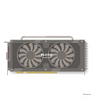
NVIDIA GeForce GTX 760 NVIDIA GeForce GTX 760
NVIDIA GeForce GTS 450 NVIDIA GeForce GTS 450
VS

Comparision NVIDIA GeForce GTX 760 vs NVIDIA GeForce GTS 450

NVIDIA GeForce GTX 760

WINNER
NVIDIA GeForce GTX 760

Rating: 15 points
NVIDIA GeForce GTS 450

NVIDIA GeForce GTS 450

Rating: 4 points
Grade
NVIDIA GeForce GTX 760
NVIDIA GeForce GTS 450
Performance
5
4
Memory
3
2
General information
7
7
Functions
8
6
Benchmark tests
2
0
Ports
7
7

Top specs and features

Passmark score

NVIDIA GeForce GTX 760: 4592 NVIDIA GeForce GTS 450: 1278

3DMark Cloud Gate GPU benchmark score

NVIDIA GeForce GTX 760: 38599 NVIDIA GeForce GTS 450: 11978

3DMark Fire Strike Score

NVIDIA GeForce GTX 760: 5221 NVIDIA GeForce GTS 450: 1408

3DMark Fire Strike Graphics test score

NVIDIA GeForce GTX 760: 5729 NVIDIA GeForce GTS 450: 1487

3DMark 11 Performance GPU benchmark score

NVIDIA GeForce GTX 760: 7655 NVIDIA GeForce GTS 450: 1817

Description

The NVIDIA GeForce GTX 760 video card is based on the Kepler architecture. NVIDIA GeForce GTS 450 on the Fermi architecture. The first has 3540 million transistors. The second is 1170 million. NVIDIA GeForce GTX 760 has a transistor size of 28 nm versus 40.

The base clock speed of the first video card is 980 MHz versus 783 MHz for the second.

Let's move on to memory. NVIDIA GeForce GTX 760 has 2 GB. NVIDIA GeForce GTS 450 has 2 GB installed. The bandwidth of the first video card is 192.3 Gb/s versus 57.73 Gb/s of the second.

FLOPS of NVIDIA GeForce GTX 760 is 2.46. At NVIDIA GeForce GTS 450 0.61.

Goes to tests in benchmarks. In the Passmark benchmark, NVIDIA GeForce GTX 760 scored 4592 points. And here is the second card 1278 points. In 3DMark, the first model scored 5729 points. Second 1487 points.

In terms of interfaces. The first video card is connected using PCIe 3.0 x16. The second is PCIe 2.0 x16. Video card NVIDIA GeForce GTX 760 has Directx version 11. Video card NVIDIA GeForce GTS 450 -- Directx version - 11.

Regarding cooling, NVIDIA GeForce GTX 760 has 170W heat dissipation requirements versus 106W for NVIDIA GeForce GTS 450.

Why NVIDIA GeForce GTX 760 is better than NVIDIA GeForce GTS 450

  • Passmark score 4592 против 1278 , more on 259%
  • 3DMark Cloud Gate GPU benchmark score 38599 против 11978 , more on 222%
  • 3DMark Fire Strike Score 5221 против 1408 , more on 271%
  • 3DMark Fire Strike Graphics test score 5729 против 1487 , more on 285%
  • 3DMark 11 Performance GPU benchmark score 7655 против 1817 , more on 321%
  • 3DMark Vantage Performance test score 27951 против 9391 , more on 198%
  • GPU base clock speed 980 MHz против 783 MHz, more on 25%
  • RAM 2 GB против 1 GB, more on 100%

NVIDIA GeForce GTX 760 vs NVIDIA GeForce GTS 450: highlights

NVIDIA GeForce GTX 760
NVIDIA GeForce GTS 450
Performance
GPU base clock speed
The graphics processing unit (GPU) has a high clock speed.
980 MHz
max 2457
Average: 1124.9 MHz
783 MHz
max 2457
Average: 1124.9 MHz
Gpu memory speed
This is an important aspect for calculating memory bandwidth.
1502 MHz
max 16000
Average: 1468 MHz
902 MHz
max 16000
Average: 1468 MHz
FLOPS
Measuring the processing power of a processor is called FLOPS.
2.46 TFLOPS
max 1142.32
Average: 53 TFLOPS
0.61 TFLOPS
max 1142.32
Average: 53 TFLOPS
RAM
RAM in video cards (also known as video memory or VRAM) is a special type of memory used by a video card to store graphics data. It serves as a temporary buffer for textures, shaders, geometry, and other graphics resources that are needed to display images on the screen. More RAM allows the graphics card to work with more data and handle more complex graphic scenes with high resolution and detail. Show more
2 GB
max 128
Average: 4.6 GB
1 GB
max 128
Average: 4.6 GB
Number of PCIe lanes
The number of PCIe lanes in video cards determines the speed and bandwidth of data transfer between the video card and other computer components through the PCIe interface. The more PCIe lanes a video card has, the more bandwidth and ability to communicate with other computer components. Show more
16
max 16
Average:
16
max 16
Average:
L1 cache size
The amount of L1 cache in video cards is usually small and is measured in kilobytes (KB) or megabytes (MB). It is designed to temporarily store the most active and frequently used data and instructions, allowing the graphics card to access them faster and reduce delays in graphics operations. Show more
16
64
Pixel rendering speed
The higher the pixel rendering speed, the smoother and more realistic the display of graphics and the movement of objects on the screen will be.
25 GTexel/s    
max 563
Average: 94.3 GTexel/s    
6.26 GTexel/s    
max 563
Average: 94.3 GTexel/s    
TMUs
Responsible for texturing objects in 3D graphics. TMU provides textures to the surfaces of objects, which gives them a realistic look and detail. The number of TMUs in a video card determines its ability to process textures. The more TMUs, the more textures can be processed at the same time, which contributes to better texturing of objects and increases the realism of graphics. Show more
96
max 880
Average: 140.1
32
max 880
Average: 140.1
ROPs
Responsible for the final processing of pixels and their display on the screen. ROPs perform various operations on pixels, such as blending colors, applying transparency, and writing to the framebuffer. The number of ROPs in a video card affects its ability to process and display graphics. The more ROPs, the more pixels and image fragments can be processed and displayed on the screen at the same time. A higher number of ROPs generally results in faster and more efficient graphics rendering and better performance in games and graphics applications. Show more
32
max 256
Average: 56.8
16
max 256
Average: 56.8
Number of shader blocks
The number of shader units in video cards refers to the number of parallel processors that perform computational operations in the GPU. The more shader units in the video card, the more computing resources are available for processing graphics tasks. Show more
1152
max 17408
Average:
192
max 17408
Average:
L2 cache size
Used to temporarily store data and instructions used by the graphics card when performing graphics calculations. A larger L2 cache allows the graphics card to store more data and instructions, which helps speed up the processing of graphics operations. Show more
512
256
Turbo gpu
If the GPU speed has dropped below its limit, then to improve performance, it can go to a high clock speed.
1032 MHz
max 2903
Average: 1514 MHz
MHz
max 2903
Average: 1514 MHz
Texture size
A certain number of textured pixels are displayed on the screen every second.
94.1 GTexels/s
max 756.8
Average: 145.4 GTexels/s
25.1 GTexels/s
max 756.8
Average: 145.4 GTexels/s
architecture name
Kepler
Fermi
GPU name
GK104
GF106
Memory
Memory bandwidth
This is the rate at which the device stores or reads information.
192.3 GB/s
max 2656
Average: 257.8 GB/s
57.73 GB/s
max 2656
Average: 257.8 GB/s
Effective memory speed
The effective memory clock is calculated from the size and transfer rate of the memory information. The performance of the device in applications depends on the clock frequency. The higher it is, the better. Show more
6008 MHz
max 19500
Average: 6984.5 MHz
3608 MHz
max 19500
Average: 6984.5 MHz
RAM
RAM in video cards (also known as video memory or VRAM) is a special type of memory used by a video card to store graphics data. It serves as a temporary buffer for textures, shaders, geometry, and other graphics resources that are needed to display images on the screen. More RAM allows the graphics card to work with more data and handle more complex graphic scenes with high resolution and detail. Show more
2 GB
max 128
Average: 4.6 GB
1 GB
max 128
Average: 4.6 GB
GDDR memory versions
Latest versions of GDDR memory provide high data transfer rates to improve overall performance
5
max 6
Average: 4.9
5
max 6
Average: 4.9
Memory bus width
A wide memory bus means that it can transfer more information in one cycle. This property affects memory performance as well as the overall performance of the device's graphics card. Show more
256 bit
max 8192
Average: 283.9 bit
128 bit
max 8192
Average: 283.9 bit
General information
Crystal size
The physical dimensions of the chip on which the transistors, microcircuits and other components necessary for the operation of the video card are located. The larger the die size, the more space the GPU takes up on the graphics card. Larger die sizes can provide more computing resources such as CUDA cores or tensor cores, which can result in increased performance and graphics processing capabilities. Show more
294
max 826
Average: 356.7
238
max 826
Average: 356.7
Length
240
max 524
Average: 250.2
210
max 524
Average: 250.2
Generation
A new generation of graphics card usually includes improved architecture, higher performance, more efficient use of power, improved graphics capabilities, and new features. Show more
GeForce 700
GeForce 400
Manufacturer
TSMC
TSMC
Power supply power
When choosing a power supply for a video card, you must take into account the power requirements of the video card manufacturer, as well as other computer components. Show more
450
max 1300
Average:
300
max 1300
Average:
Year of issue
2013
max 2023
Average:
2010
max 2023
Average:
Power Consumption (TDP)
Heat Dissipation Requirements (TDP) is the maximum possible amount of energy dissipated by the cooling system. The lower the TDP, the less power will be consumed Show more
170 W
Average: 160 W
106 W
Average: 160 W
Technological process
The small size of the semiconductors means this is a new generation chip.
28 nm
Average: 34.7 nm
40 nm
Average: 34.7 nm
Number of transistors
The higher their number, the more processor power this indicates.
3540 million
max 80000
Average: 7150 million
1170 million
max 80000
Average: 7150 million
PCIe connection interface
A considerable speed of the expansion card used to connect the computer to the peripherals is provided. The updated versions offer impressive bandwidth and high performance. Show more
3
max 4
Average: 3
2
max 4
Average: 3
Purpose
Desktop
Desktop
Price at the time of release
249 $
max 419999
Average: 5679.5 $
129 $
max 419999
Average: 5679.5 $
Functions
OpenGL Version
OpenGL provides access to the graphics card's hardware capabilities for displaying 2D and 3D graphics objects. New versions of OpenGL may include support for new graphical effects, performance optimizations, bug fixes, and other improvements. Show more
4.6
max 4.6
Average:
4.6
max 4.6
Average:
DirectX
Used in demanding games, providing improved graphics
11
max 12.2
Average: 11.4
11
max 12.2
Average: 11.4
Shader model version
The higher the version of the shader model in the video card, the more functions and possibilities are available for programming graphic effects.
5.1
max 6.7
Average: 5.9
5.1
max 6.7
Average: 5.9
Vulkan version
A higher version of Vulkan usually means a larger set of features, optimizations, and enhancements that software developers can use to create better and more realistic graphical applications and games. Show more
1.2
max 1.3
Average:
max 1.3
Average:
CUDA Version
Allows you to use the compute cores of your graphics card to perform parallel computing, which can be useful in areas such as scientific research, deep learning, image processing, and other computationally intensive tasks. Show more
3
max 9
Average:
2.1
max 9
Average:
Benchmark tests
Passmark score
The Passmark Video Card Test is a program for measuring and comparing the performance of a graphics system. It conducts various tests and calculations to evaluate the speed and performance of a graphics card in various areas. Show more
4592
max 30117
Average: 7628.6
1278
max 30117
Average: 7628.6
3DMark Cloud Gate GPU benchmark score
38599
max 196940
Average: 80042.3
11978
max 196940
Average: 80042.3
3DMark Fire Strike Score
5221
max 39424
Average: 12463
1408
max 39424
Average: 12463
3DMark Fire Strike Graphics test score
It measures and compares the ability of a graphics card to handle high-resolution 3D graphics with various graphical effects. The Fire Strike Graphics test includes complex scenes, lighting, shadows, particles, reflections, and other graphical effects to evaluate the graphics card's performance in gaming and other demanding graphics scenarios. Show more
5729
max 51062
Average: 11859.1
1487
max 51062
Average: 11859.1
3DMark 11 Performance GPU benchmark score
7655
max 59675
Average: 18799.9
1817
max 59675
Average: 18799.9
3DMark Vantage Performance test score
27951
max 97329
Average: 37830.6
9391
max 97329
Average: 37830.6
Unigine Heaven 3.0 test score
73
max 61874
Average: 2402
max 61874
Average: 2402
Unigine Heaven 4.0 test score
During the Unigine Heaven test, the graphics card goes through a series of graphical tasks and effects that can be intensive to process, and displays the result as a numerical value (points) and a visual representation of the scene. Show more
818
max 4726
Average: 1291.1
max 4726
Average: 1291.1
Octane Render test score OctaneBench
A special test that is used to evaluate the performance of video cards in rendering using the Octane Render engine.
42
max 128
Average: 47.1
15
max 128
Average: 47.1
Ports
Has hdmi output
HDMI output allows you to connect devices with HDMI or mini HDMI ports. They can send video and audio to the display.
Available
Available
HDMI version
The latest version provides a wide signal transmission channel due to the increased number of audio channels, frames per second, etc.
1.4
max 2.1
Average: 1.9
1.3
max 2.1
Average: 1.9
DisplayPort
Allows you to connect to a display using DisplayPort
1
max 4
Average: 2.2
max 4
Average: 2.2
DVI Outputs
Allows you to connect to a display using DVI
2
max 3
Average: 1.4
2
max 3
Average: 1.4
Number of HDMI connectors
The more their number, the more devices can be connected at the same time (for example, game / TV set-top boxes)
1
max 3
Average: 1.1
max 3
Average: 1.1
Interface
PCIe 3.0 x16
PCIe 2.0 x16
HDMI
A digital interface that is used to transmit high-resolution audio and video signals.
Available
Available

FAQ

How does the NVIDIA GeForce GTX 760 processor perform in benchmarks?

Passmark NVIDIA GeForce GTX 760 scored 4592 points. The second video card scored 1278 points in Passmark.

What FLOPS do video cards have?

FLOPS NVIDIA GeForce GTX 760 is 2.46 TFLOPS. But the second video card has FLOPS equal to 0.61 TFLOPS.

What power consumption?

NVIDIA GeForce GTX 760 170 Watt. NVIDIA GeForce GTS 450 106 Watt.

How fast are NVIDIA GeForce GTX 760 and NVIDIA GeForce GTS 450?

NVIDIA GeForce GTX 760 operates at 980 MHz. In this case, the maximum frequency reaches 1032 MHz. The clock base frequency of NVIDIA GeForce GTS 450 reaches 783 MHz. In turbo mode it reaches There is no data MHz.

What kind of memory do graphics cards have?

NVIDIA GeForce GTX 760 supports GDDR5. Installed 2 GB of RAM. Throughput reaches 192.3 GB/s. NVIDIA GeForce GTS 450 works with GDDR5. The second one has 1 GB of RAM installed. Its bandwidth is 192.3 GB/s.

How many HDMI connectors do they have?

NVIDIA GeForce GTX 760 has 1 HDMI outputs. NVIDIA GeForce GTS 450 is equipped with There is no data HDMI outputs.

What power connectors are used?

NVIDIA GeForce GTX 760 uses There is no data. NVIDIA GeForce GTS 450 is equipped with There is no data HDMI outputs.

What architecture are video cards based on?

NVIDIA GeForce GTX 760 is built on Kepler. NVIDIA GeForce GTS 450 uses the Fermi architecture.

What graphics processor is being used?

NVIDIA GeForce GTX 760 is equipped with GK104. NVIDIA GeForce GTS 450 is set to GF106.

How many PCIe lanes

The first graphics card has 16 PCIe lanes. And the PCIe version is 3. NVIDIA GeForce GTS 450 16 PCIe lanes. PCIe version 3.

How many transistors?

NVIDIA GeForce GTX 760 has 3540 million transistors. NVIDIA GeForce GTS 450 has 1170 million transistors