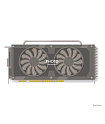
EVGA GeForce GTX 1050 SC ACX 2.0 EVGA GeForce GTX 1050 SC ACX 2.0
EVGA GeForce GTX 1050 SSC ACX 3.0 EVGA GeForce GTX 1050 SSC ACX 3.0
VS

Comparision EVGA GeForce GTX 1050 SC ACX 2.0 vs EVGA GeForce GTX 1050 SSC ACX 3.0

EVGA GeForce GTX 1050 SC ACX 2.0

WINNER
EVGA GeForce GTX 1050 SC ACX 2.0

Rating: 17 points
Grade
EVGA GeForce GTX 1050 SC ACX 2.0
EVGA GeForce GTX 1050 SSC ACX 3.0
Performance
6
6
Memory
3
3
General information
7
7
Functions
7
7
Benchmark tests
2
2
Ports
4
4

Top specs and features

Passmark score

EVGA GeForce GTX 1050 SC ACX 2.0: 5193 EVGA GeForce GTX 1050 SSC ACX 3.0: 4929

3DMark Cloud Gate GPU benchmark score

EVGA GeForce GTX 1050 SC ACX 2.0: 40986 EVGA GeForce GTX 1050 SSC ACX 3.0: 38901

3DMark Fire Strike Score

EVGA GeForce GTX 1050 SC ACX 2.0: 6132 EVGA GeForce GTX 1050 SSC ACX 3.0: 5820

3DMark Fire Strike Graphics test score

EVGA GeForce GTX 1050 SC ACX 2.0: 6808 EVGA GeForce GTX 1050 SSC ACX 3.0: 6461

3DMark 11 Performance GPU benchmark score

EVGA GeForce GTX 1050 SC ACX 2.0: 8585 EVGA GeForce GTX 1050 SSC ACX 3.0: 8148

Description

The EVGA GeForce GTX 1050 SC ACX 2.0 video card is based on the Pascal architecture. EVGA GeForce GTX 1050 SSC ACX 3.0 on the Pascal architecture. The first has 3300 million transistors. The second is 3300 million. EVGA GeForce GTX 1050 SC ACX 2.0 has a transistor size of 14 nm versus 14.

The base clock speed of the first video card is 1417 MHz versus 1430 MHz for the second.

Let's move on to memory. EVGA GeForce GTX 1050 SC ACX 2.0 has 2 GB. EVGA GeForce GTX 1050 SSC ACX 3.0 has 2 GB installed. The bandwidth of the first video card is 112.1 Gb/s versus 112.1 Gb/s of the second.

FLOPS of EVGA GeForce GTX 1050 SC ACX 2.0 is 1.74. At EVGA GeForce GTX 1050 SSC ACX 3.0 1.76.

Goes to tests in benchmarks. In the Passmark benchmark, EVGA GeForce GTX 1050 SC ACX 2.0 scored 5193 points. And here is the second card 4929 points. In 3DMark, the first model scored 6808 points. Second 6461 points.

In terms of interfaces. The first video card is connected using PCIe 3.0 x16. The second is PCIe 3.0 x16. Video card EVGA GeForce GTX 1050 SC ACX 2.0 has Directx version 12. Video card EVGA GeForce GTX 1050 SSC ACX 3.0 -- Directx version - 12.

Regarding cooling, EVGA GeForce GTX 1050 SC ACX 2.0 has 75W heat dissipation requirements versus 75W for EVGA GeForce GTX 1050 SSC ACX 3.0.

Why EVGA GeForce GTX 1050 SC ACX 2.0 is better than EVGA GeForce GTX 1050 SSC ACX 3.0

  • Passmark score 5193 против 4929 , more on 5%
  • 3DMark Cloud Gate GPU benchmark score 40986 против 38901 , more on 5%
  • 3DMark Fire Strike Score 6132 против 5820 , more on 5%
  • 3DMark Fire Strike Graphics test score 6808 против 6461 , more on 5%
  • 3DMark 11 Performance GPU benchmark score 8585 против 8148 , more on 5%
  • 3DMark Vantage Performance test score 32514 против 30860 , more on 5%
  • 3DMark Ice Storm GPU benchmark score 350228 против 332408 , more on 5%
  • Unigine Heaven 3.0 test score 88 против 83 , more on 6%

EVGA GeForce GTX 1050 SC ACX 2.0 vs EVGA GeForce GTX 1050 SSC ACX 3.0: highlights

EVGA GeForce GTX 1050 SC ACX 2.0
EVGA GeForce GTX 1050 SSC ACX 3.0
Performance
GPU base clock speed
The graphics processing unit (GPU) has a high clock speed.
1417 MHz
max 2457
Average: 1124.9 MHz
1430 MHz
max 2457
Average: 1124.9 MHz
Gpu memory speed
This is an important aspect for calculating memory bandwidth.
1752 MHz
max 16000
Average: 1468 MHz
1752 MHz
max 16000
Average: 1468 MHz
FLOPS
Measuring the processing power of a processor is called FLOPS.
1.74 TFLOPS
max 1142.32
Average: 53 TFLOPS
1.76 TFLOPS
max 1142.32
Average: 53 TFLOPS
RAM
RAM in video cards (also known as video memory or VRAM) is a special type of memory used by a video card to store graphics data. It serves as a temporary buffer for textures, shaders, geometry, and other graphics resources that are needed to display images on the screen. More RAM allows the graphics card to work with more data and handle more complex graphic scenes with high resolution and detail. Show more
2 GB
max 128
Average: 4.6 GB
2 GB
max 128
Average: 4.6 GB
Number of PCIe lanes
The number of PCIe lanes in video cards determines the speed and bandwidth of data transfer between the video card and other computer components through the PCIe interface. The more PCIe lanes a video card has, the more bandwidth and ability to communicate with other computer components. Show more
16
max 16
Average:
16
max 16
Average:
L1 cache size
The amount of L1 cache in video cards is usually small and is measured in kilobytes (KB) or megabytes (MB). It is designed to temporarily store the most active and frequently used data and instructions, allowing the graphics card to access them faster and reduce delays in graphics operations. Show more
48
48
Pixel rendering speed
The higher the pixel rendering speed, the smoother and more realistic the display of graphics and the movement of objects on the screen will be.
45.3 GTexel/s    
max 563
Average: 94.3 GTexel/s    
45.8 GTexel/s    
max 563
Average: 94.3 GTexel/s    
ROPs
Responsible for the final processing of pixels and their display on the screen. ROPs perform various operations on pixels, such as blending colors, applying transparency, and writing to the framebuffer. The number of ROPs in a video card affects its ability to process and display graphics. The more ROPs, the more pixels and image fragments can be processed and displayed on the screen at the same time. A higher number of ROPs generally results in faster and more efficient graphics rendering and better performance in games and graphics applications. Show more
32
max 256
Average: 56.8
32
max 256
Average: 56.8
Number of shader blocks
The number of shader units in video cards refers to the number of parallel processors that perform computational operations in the GPU. The more shader units in the video card, the more computing resources are available for processing graphics tasks. Show more
640
max 17408
Average:
640
max 17408
Average:
Turbo gpu
If the GPU speed has dropped below its limit, then to improve performance, it can go to a high clock speed.
1531 MHz
max 2903
Average: 1514 MHz
1544 MHz
max 2903
Average: 1514 MHz
Texture size
A certain number of textured pixels are displayed on the screen every second.
56.7 GTexels/s
max 756.8
Average: 145.4 GTexels/s
57.2 GTexels/s
max 756.8
Average: 145.4 GTexels/s
architecture name
Pascal
Pascal
GPU name
N17P-G1
N17P-G1
Memory
Memory bandwidth
This is the rate at which the device stores or reads information.
112.1 GB/s
max 2656
Average: 257.8 GB/s
112.1 GB/s
max 2656
Average: 257.8 GB/s
Effective memory speed
The effective memory clock is calculated from the size and transfer rate of the memory information. The performance of the device in applications depends on the clock frequency. The higher it is, the better. Show more
7008 MHz
max 19500
Average: 6984.5 MHz
7008 MHz
max 19500
Average: 6984.5 MHz
RAM
RAM in video cards (also known as video memory or VRAM) is a special type of memory used by a video card to store graphics data. It serves as a temporary buffer for textures, shaders, geometry, and other graphics resources that are needed to display images on the screen. More RAM allows the graphics card to work with more data and handle more complex graphic scenes with high resolution and detail. Show more
2 GB
max 128
Average: 4.6 GB
2 GB
max 128
Average: 4.6 GB
GDDR memory versions
Latest versions of GDDR memory provide high data transfer rates to improve overall performance
5
max 6
Average: 4.9
5
max 6
Average: 4.9
Memory bus width
A wide memory bus means that it can transfer more information in one cycle. This property affects memory performance as well as the overall performance of the device's graphics card. Show more
128 bit
max 8192
Average: 283.9 bit
128 bit
max 8192
Average: 283.9 bit
General information
Crystal size
The physical dimensions of the chip on which the transistors, microcircuits and other components necessary for the operation of the video card are located. The larger the die size, the more space the GPU takes up on the graphics card. Larger die sizes can provide more computing resources such as CUDA cores or tensor cores, which can result in increased performance and graphics processing capabilities. Show more
132
max 826
Average: 356.7
132
max 826
Average: 356.7
Generation
A new generation of graphics card usually includes improved architecture, higher performance, more efficient use of power, improved graphics capabilities, and new features. Show more
GeForce 10
GeForce 10
Manufacturer
Samsung
Samsung
Power Consumption (TDP)
Heat Dissipation Requirements (TDP) is the maximum possible amount of energy dissipated by the cooling system. The lower the TDP, the less power will be consumed Show more
75 W
Average: 160 W
75 W
Average: 160 W
Technological process
The small size of the semiconductors means this is a new generation chip.
14 nm
Average: 34.7 nm
14 nm
Average: 34.7 nm
Number of transistors
The higher their number, the more processor power this indicates.
3300 million
max 80000
Average: 7150 million
3300 million
max 80000
Average: 7150 million
PCIe connection interface
A considerable speed of the expansion card used to connect the computer to the peripherals is provided. The updated versions offer impressive bandwidth and high performance. Show more
3
max 4
Average: 3
3
max 4
Average: 3
Width
144.8 mm
max 421.7
Average: 192.1 mm
228.6 mm
max 421.7
Average: 192.1 mm
Height
111.1 mm
max 620
Average: 89.6 mm
111.1 mm
max 620
Average: 89.6 mm
Purpose
Desktop
Desktop
Functions
OpenGL Version
OpenGL provides access to the graphics card's hardware capabilities for displaying 2D and 3D graphics objects. New versions of OpenGL may include support for new graphical effects, performance optimizations, bug fixes, and other improvements. Show more
4.5
max 4.6
Average:
4.5
max 4.6
Average:
DirectX
Used in demanding games, providing improved graphics
12
max 12.2
Average: 11.4
12
max 12.2
Average: 11.4
Shader model version
The higher the version of the shader model in the video card, the more functions and possibilities are available for programming graphic effects.
6.4
max 6.7
Average: 5.9
6.4
max 6.7
Average: 5.9
Vulkan version
A higher version of Vulkan usually means a larger set of features, optimizations, and enhancements that software developers can use to create better and more realistic graphical applications and games. Show more
1.3
max 1.3
Average:
1.3
max 1.3
Average:
CUDA Version
Allows you to use the compute cores of your graphics card to perform parallel computing, which can be useful in areas such as scientific research, deep learning, image processing, and other computationally intensive tasks. Show more
6.1
max 9
Average:
6.1
max 9
Average:
Benchmark tests
Passmark score
The Passmark Video Card Test is a program for measuring and comparing the performance of a graphics system. It conducts various tests and calculations to evaluate the speed and performance of a graphics card in various areas. Show more
5193
max 30117
Average: 7628.6
4929
max 30117
Average: 7628.6
3DMark Cloud Gate GPU benchmark score
40986
max 196940
Average: 80042.3
38901
max 196940
Average: 80042.3
3DMark Fire Strike Score
6132
max 39424
Average: 12463
5820
max 39424
Average: 12463
3DMark Fire Strike Graphics test score
It measures and compares the ability of a graphics card to handle high-resolution 3D graphics with various graphical effects. The Fire Strike Graphics test includes complex scenes, lighting, shadows, particles, reflections, and other graphical effects to evaluate the graphics card's performance in gaming and other demanding graphics scenarios. Show more
6808
max 51062
Average: 11859.1
6461
max 51062
Average: 11859.1
3DMark 11 Performance GPU benchmark score
8585
max 59675
Average: 18799.9
8148
max 59675
Average: 18799.9
3DMark Vantage Performance test score
32514
max 97329
Average: 37830.6
30860
max 97329
Average: 37830.6
3DMark Ice Storm GPU benchmark score
350228
max 539757
Average: 372425.7
332408
max 539757
Average: 372425.7
Unigine Heaven 3.0 test score
88
max 61874
Average: 2402
83
max 61874
Average: 2402
Ports
Has hdmi output
HDMI output allows you to connect devices with HDMI or mini HDMI ports. They can send video and audio to the display.
Available
Available
HDMI version
The latest version provides a wide signal transmission channel due to the increased number of audio channels, frames per second, etc.
2
max 2.1
Average: 1.9
2
max 2.1
Average: 1.9
DisplayPort
Allows you to connect to a display using DisplayPort
1
max 4
Average: 2.2
1
max 4
Average: 2.2
DVI Outputs
Allows you to connect to a display using DVI
1
max 3
Average: 1.4
1
max 3
Average: 1.4
Number of HDMI connectors
The more their number, the more devices can be connected at the same time (for example, game / TV set-top boxes)
1
max 3
Average: 1.1
1
max 3
Average: 1.1
Interface
PCIe 3.0 x16
PCIe 3.0 x16
HDMI
A digital interface that is used to transmit high-resolution audio and video signals.
Available
Available

FAQ

How does the EVGA GeForce GTX 1050 SC ACX 2.0 processor perform in benchmarks?

Passmark EVGA GeForce GTX 1050 SC ACX 2.0 scored 5193 points. The second video card scored 4929 points in Passmark.

What FLOPS do video cards have?

FLOPS EVGA GeForce GTX 1050 SC ACX 2.0 is 1.74 TFLOPS. But the second video card has FLOPS equal to 1.76 TFLOPS.

What power consumption?

EVGA GeForce GTX 1050 SC ACX 2.0 75 Watt. EVGA GeForce GTX 1050 SSC ACX 3.0 75 Watt.

How fast are EVGA GeForce GTX 1050 SC ACX 2.0 and EVGA GeForce GTX 1050 SSC ACX 3.0?

EVGA GeForce GTX 1050 SC ACX 2.0 operates at 1417 MHz. In this case, the maximum frequency reaches 1531 MHz. The clock base frequency of EVGA GeForce GTX 1050 SSC ACX 3.0 reaches 1430 MHz. In turbo mode it reaches 1544 MHz.

What kind of memory do graphics cards have?

EVGA GeForce GTX 1050 SC ACX 2.0 supports GDDR5. Installed 2 GB of RAM. Throughput reaches 112.1 GB/s. EVGA GeForce GTX 1050 SSC ACX 3.0 works with GDDR5. The second one has 2 GB of RAM installed. Its bandwidth is 112.1 GB/s.

How many HDMI connectors do they have?

EVGA GeForce GTX 1050 SC ACX 2.0 has 1 HDMI outputs. EVGA GeForce GTX 1050 SSC ACX 3.0 is equipped with 1 HDMI outputs.

What power connectors are used?

EVGA GeForce GTX 1050 SC ACX 2.0 uses There is no data. EVGA GeForce GTX 1050 SSC ACX 3.0 is equipped with There is no data HDMI outputs.

What architecture are video cards based on?

EVGA GeForce GTX 1050 SC ACX 2.0 is built on Pascal. EVGA GeForce GTX 1050 SSC ACX 3.0 uses the Pascal architecture.

What graphics processor is being used?

EVGA GeForce GTX 1050 SC ACX 2.0 is equipped with N17P-G1. EVGA GeForce GTX 1050 SSC ACX 3.0 is set to N17P-G1.

How many PCIe lanes

The first graphics card has 16 PCIe lanes. And the PCIe version is 3. EVGA GeForce GTX 1050 SSC ACX 3.0 16 PCIe lanes. PCIe version 3.

How many transistors?

EVGA GeForce GTX 1050 SC ACX 2.0 has 3300 million transistors. EVGA GeForce GTX 1050 SSC ACX 3.0 has 3300 million transistors