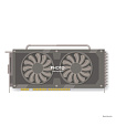
Sapphire Nitro+ Radeon RX 5700 XT Sapphire Nitro+ Radeon RX 5700 XT
AMD Radeon R9 290X AMD Radeon R9 290X
VS

Comparision Sapphire Nitro+ Radeon RX 5700 XT vs AMD Radeon R9 290X

Sapphire Nitro+ Radeon RX 5700 XT

WINNER
Sapphire Nitro+ Radeon RX 5700 XT

Rating: 54 points
AMD Radeon R9 290X

AMD Radeon R9 290X

Rating: 24 points
Grade
Sapphire Nitro+ Radeon RX 5700 XT
AMD Radeon R9 290X
Performance
7
5
Memory
6
3
General information
5
7
Functions
7
8
Benchmark tests
5
2
Ports
4
7

Top specs and features

Passmark score

Sapphire Nitro+ Radeon RX 5700 XT: 16231 AMD Radeon R9 290X: 7175

3DMark Cloud Gate GPU benchmark score

Sapphire Nitro+ Radeon RX 5700 XT: 136081 AMD Radeon R9 290X: 71492

3DMark Fire Strike Score

Sapphire Nitro+ Radeon RX 5700 XT: 21339 AMD Radeon R9 290X: 9503

3DMark Fire Strike Graphics test score

Sapphire Nitro+ Radeon RX 5700 XT: 24515 AMD Radeon R9 290X: 11322

3DMark 11 Performance GPU benchmark score

Sapphire Nitro+ Radeon RX 5700 XT: 34308 AMD Radeon R9 290X: 15623

Description

The Sapphire Nitro+ Radeon RX 5700 XT video card is based on the Navi / RDNA architecture. AMD Radeon R9 290X on the GCN 2.0 architecture. The first has 10300 million transistors. The second is 6200 million. Sapphire Nitro+ Radeon RX 5700 XT has a transistor size of 7 nm versus 28.

The base clock speed of the first video card is 1770 MHz versus 1000 MHz for the second.

Let's move on to memory. Sapphire Nitro+ Radeon RX 5700 XT has 8 GB. AMD Radeon R9 290X has 8 GB installed. The bandwidth of the first video card is 448 Gb/s versus 320 Gb/s of the second.

FLOPS of Sapphire Nitro+ Radeon RX 5700 XT is 9.84. At AMD Radeon R9 290X 5.5.

Goes to tests in benchmarks. In the Passmark benchmark, Sapphire Nitro+ Radeon RX 5700 XT scored 16231 points. And here is the second card 7175 points. In 3DMark, the first model scored 24515 points. Second 11322 points.

In terms of interfaces. The first video card is connected using PCIe 4.0 x16. The second is PCIe 3.0 x16. Video card Sapphire Nitro+ Radeon RX 5700 XT has Directx version 12. Video card AMD Radeon R9 290X -- Directx version - 12.

Regarding cooling, Sapphire Nitro+ Radeon RX 5700 XT has 225W heat dissipation requirements versus 290W for AMD Radeon R9 290X.

Why Sapphire Nitro+ Radeon RX 5700 XT is better than AMD Radeon R9 290X

  • Passmark score 16231 против 7175 , more on 126%
  • 3DMark Cloud Gate GPU benchmark score 136081 против 71492 , more on 90%
  • 3DMark Fire Strike Score 21339 против 9503 , more on 125%
  • 3DMark Fire Strike Graphics test score 24515 против 11322 , more on 117%
  • 3DMark 11 Performance GPU benchmark score 34308 против 15623 , more on 120%
  • 3DMark Vantage Performance test score 64065 против 36026 , more on 78%
  • 3DMark Ice Storm GPU benchmark score 439840 против 320845 , more on 37%
  • GPU base clock speed 1770 MHz против 1000 MHz, more on 77%

Sapphire Nitro+ Radeon RX 5700 XT vs AMD Radeon R9 290X: highlights

Sapphire Nitro+ Radeon RX 5700 XT
AMD Radeon R9 290X
AMD Radeon R9 290X
Performance
GPU base clock speed
The graphics processing unit (GPU) has a high clock speed.
1770 MHz
max 2457
Average: 1124.9 MHz
1000 MHz
max 2457
Average: 1124.9 MHz
Gpu memory speed
This is an important aspect for calculating memory bandwidth.
1750 MHz
max 16000
Average: 1468 MHz
1250 MHz
max 16000
Average: 1468 MHz
FLOPS
Measuring the processing power of a processor is called FLOPS.
9.84 TFLOPS
max 1142.32
Average: 53 TFLOPS
5.5 TFLOPS
max 1142.32
Average: 53 TFLOPS
RAM
RAM in video cards (also known as video memory or VRAM) is a special type of memory used by a video card to store graphics data. It serves as a temporary buffer for textures, shaders, geometry, and other graphics resources that are needed to display images on the screen. More RAM allows the graphics card to work with more data and handle more complex graphic scenes with high resolution and detail. Show more
8 GB
max 128
Average: 4.6 GB
4 GB
max 128
Average: 4.6 GB
Number of PCIe lanes
The number of PCIe lanes in video cards determines the speed and bandwidth of data transfer between the video card and other computer components through the PCIe interface. The more PCIe lanes a video card has, the more bandwidth and ability to communicate with other computer components. Show more
16
max 16
Average:
16
max 16
Average:
Pixel rendering speed
The higher the pixel rendering speed, the smoother and more realistic the display of graphics and the movement of objects on the screen will be.
128.6 GTexel/s    
max 563
Average: 94.3 GTexel/s    
64 GTexel/s    
max 563
Average: 94.3 GTexel/s    
TMUs
Responsible for texturing objects in 3D graphics. TMU provides textures to the surfaces of objects, which gives them a realistic look and detail. The number of TMUs in a video card determines its ability to process textures. The more TMUs, the more textures can be processed at the same time, which contributes to better texturing of objects and increases the realism of graphics. Show more
160
max 880
Average: 140.1
176
max 880
Average: 140.1
ROPs
Responsible for the final processing of pixels and their display on the screen. ROPs perform various operations on pixels, such as blending colors, applying transparency, and writing to the framebuffer. The number of ROPs in a video card affects its ability to process and display graphics. The more ROPs, the more pixels and image fragments can be processed and displayed on the screen at the same time. A higher number of ROPs generally results in faster and more efficient graphics rendering and better performance in games and graphics applications. Show more
64
max 256
Average: 56.8
64
max 256
Average: 56.8
Number of shader blocks
The number of shader units in video cards refers to the number of parallel processors that perform computational operations in the GPU. The more shader units in the video card, the more computing resources are available for processing graphics tasks. Show more
2560
max 17408
Average:
2816
max 17408
Average:
L2 cache size
Used to temporarily store data and instructions used by the graphics card when performing graphics calculations. A larger L2 cache allows the graphics card to store more data and instructions, which helps speed up the processing of graphics operations. Show more
4000
1024
Turbo gpu
If the GPU speed has dropped below its limit, then to improve performance, it can go to a high clock speed.
2010 MHz
max 2903
Average: 1514 MHz
MHz
max 2903
Average: 1514 MHz
Texture size
A certain number of textured pixels are displayed on the screen every second.
321.6 GTexels/s
max 756.8
Average: 145.4 GTexels/s
141 GTexels/s
max 756.8
Average: 145.4 GTexels/s
architecture name
Navi / RDNA
GCN 2.0
GPU name
Navi 10
Hawaii
Memory
Memory bandwidth
This is the rate at which the device stores or reads information.
448 GB/s
max 2656
Average: 257.8 GB/s
320 GB/s
max 2656
Average: 257.8 GB/s
Effective memory speed
The effective memory clock is calculated from the size and transfer rate of the memory information. The performance of the device in applications depends on the clock frequency. The higher it is, the better. Show more
14000 MHz
max 19500
Average: 6984.5 MHz
5000 MHz
max 19500
Average: 6984.5 MHz
RAM
RAM in video cards (also known as video memory or VRAM) is a special type of memory used by a video card to store graphics data. It serves as a temporary buffer for textures, shaders, geometry, and other graphics resources that are needed to display images on the screen. More RAM allows the graphics card to work with more data and handle more complex graphic scenes with high resolution and detail. Show more
8 GB
max 128
Average: 4.6 GB
4 GB
max 128
Average: 4.6 GB
GDDR memory versions
Latest versions of GDDR memory provide high data transfer rates to improve overall performance
6
max 6
Average: 4.9
5
max 6
Average: 4.9
Memory bus width
A wide memory bus means that it can transfer more information in one cycle. This property affects memory performance as well as the overall performance of the device's graphics card. Show more
256 bit
max 8192
Average: 283.9 bit
512 bit
max 8192
Average: 283.9 bit
General information
Crystal size
The physical dimensions of the chip on which the transistors, microcircuits and other components necessary for the operation of the video card are located. The larger the die size, the more space the GPU takes up on the graphics card. Larger die sizes can provide more computing resources such as CUDA cores or tensor cores, which can result in increased performance and graphics processing capabilities. Show more
251
max 826
Average: 356.7
438
max 826
Average: 356.7
Generation
A new generation of graphics card usually includes improved architecture, higher performance, more efficient use of power, improved graphics capabilities, and new features. Show more
Polaris
Volcanic Islands
Manufacturer
GlobalFoundries
TSMC
Power Consumption (TDP)
Heat Dissipation Requirements (TDP) is the maximum possible amount of energy dissipated by the cooling system. The lower the TDP, the less power will be consumed Show more
225 W
Average: 160 W
290 W
Average: 160 W
Technological process
The small size of the semiconductors means this is a new generation chip.
7 nm
Average: 34.7 nm
28 nm
Average: 34.7 nm
Number of transistors

The higher their number, the more processor power this indicates.
10300 million
max 80000
Average: 7150 million
6200 million
max 80000
Average: 7150 million
PCIe connection interface
A considerable speed of the expansion card used to connect the computer to the peripherals is provided. The updated versions offer impressive bandwidth and high performance. Show more
4
max 4
Average: 3
3
max 4
Average: 3
Width
306 mm
max 421.7
Average: 192.1 mm
109 mm
max 421.7
Average: 192.1 mm
Height
135 mm
max 620
Average: 89.6 mm
34 mm
max 620
Average: 89.6 mm
Functions
OpenGL Version
OpenGL provides access to the graphics card's hardware capabilities for displaying 2D and 3D graphics objects. New versions of OpenGL may include support for new graphical effects, performance optimizations, bug fixes, and other improvements. Show more
4.6
max 4.6
Average:
4.6
max 4.6
Average:
DirectX
Used in demanding games, providing improved graphics
12
max 12.2
Average: 11.4
12
max 12.2
Average: 11.4
Shader model version
The higher the version of the shader model in the video card, the more functions and possibilities are available for programming graphic effects.
6.5
max 6.7
Average: 5.9
6.3
max 6.7
Average: 5.9
Benchmark tests
Passmark score
The Passmark Video Card Test is a program for measuring and comparing the performance of a graphics system. It conducts various tests and calculations to evaluate the speed and performance of a graphics card in various areas. Show more
16231
max 30117
Average: 7628.6
7175
max 30117
Average: 7628.6
3DMark Cloud Gate GPU benchmark score
136081
max 196940
Average: 80042.3
71492
max 196940
Average: 80042.3
3DMark Fire Strike Score
21339
max 39424
Average: 12463
9503
max 39424
Average: 12463
3DMark Fire Strike Graphics test score
It measures and compares the ability of a graphics card to handle high-resolution 3D graphics with various graphical effects. The Fire Strike Graphics test includes complex scenes, lighting, shadows, particles, reflections, and other graphical effects to evaluate the graphics card's performance in gaming and other demanding graphics scenarios. Show more
24515
max 51062
Average: 11859.1
11322
max 51062
Average: 11859.1
3DMark 11 Performance GPU benchmark score
34308
max 59675
Average: 18799.9
15623
max 59675
Average: 18799.9
3DMark Vantage Performance test score
64065
max 97329
Average: 37830.6
36026
max 97329
Average: 37830.6
3DMark Ice Storm GPU benchmark score
439840
max 539757
Average: 372425.7
320845
max 539757
Average: 372425.7
SPECviewperf 12 test score - specvp12 sw-03
The sw-03 test includes visualization and modeling of objects using various graphic effects and techniques such as shadows, lighting, reflections and others. Show more
96
max 203
Average: 64
max 203
Average: 64
SPECviewperf 12 test score - specvp12 showcase-01
The showcase-01 test is a scene with complex 3D models and effects that demonstrates the capabilities of the graphics system in processing complex scenes. Show more
134
max 239
Average: 121.3
max 239
Average: 121.3
SPECviewperf 12 test score - Showcase
133
max 180
Average: 108.4
max 180
Average: 108.4
SPECviewperf 12 test score - specvp12 mediacal-01
44
max 107
Average: 39
max 107
Average: 39
SPECviewperf 12 test score - specvp12 maya-04
97
max 185
Average: 132.8
max 185
Average: 132.8
SPECviewperf 12 test score - specvp12 energy-01
12
max 21
Average: 10.7
max 21
Average: 10.7
SPECviewperf 12 test score - specvp12 creo-01
72
max 154
Average: 52.5
max 154
Average: 52.5
SPECviewperf 12 test score - specvp12 catia-04
160
max 190
Average: 91.5
max 190
Average: 91.5
SPECviewperf 12 test score - Catia
154
max 190
Average: 88.6
max 190
Average: 88.6
SPECviewperf 12 test score - specvp12 3dsmax-05
180
max 325
Average: 189.5
max 325
Average: 189.5
SPECviewperf 12 test score - 3ds Max
163
max 275
Average: 169.8
max 275
Average: 169.8
Ports
Has hdmi output
HDMI output allows you to connect devices with HDMI or mini HDMI ports. They can send video and audio to the display.
Available
Available
HDMI version
The latest version provides a wide signal transmission channel due to the increased number of audio channels, frames per second, etc.
2
max 2.1
Average: 1.9
1.4
max 2.1
Average: 1.9
DisplayPort
Allows you to connect to a display using DisplayPort
3
max 4
Average: 2.2
1
max 4
Average: 2.2
Number of HDMI connectors
The more their number, the more devices can be connected at the same time (for example, game / TV set-top boxes)
2
max 3
Average: 1.1
1
max 3
Average: 1.1
Interface
PCIe 4.0 x16
PCIe 3.0 x16
HDMI
A digital interface that is used to transmit high-resolution audio and video signals.
Available
Available

FAQ

How does the Sapphire Nitro+ Radeon RX 5700 XT processor perform in benchmarks?

Passmark Sapphire Nitro+ Radeon RX 5700 XT scored 16231 points. The second video card scored 7175 points in Passmark.

What FLOPS do video cards have?

FLOPS Sapphire Nitro+ Radeon RX 5700 XT is 9.84 TFLOPS. But the second video card has FLOPS equal to 5.5 TFLOPS.

What power consumption?

Sapphire Nitro+ Radeon RX 5700 XT 225 Watt. AMD Radeon R9 290X 290 Watt.

How fast are Sapphire Nitro+ Radeon RX 5700 XT and AMD Radeon R9 290X?

Sapphire Nitro+ Radeon RX 5700 XT operates at 1770 MHz. In this case, the maximum frequency reaches 2010 MHz. The clock base frequency of AMD Radeon R9 290X reaches 1000 MHz. In turbo mode it reaches There is no data MHz.

What kind of memory do graphics cards have?

Sapphire Nitro+ Radeon RX 5700 XT supports GDDR6. Installed 8 GB of RAM. Throughput reaches 448 GB/s. AMD Radeon R9 290X works with GDDR5. The second one has 4 GB of RAM installed. Its bandwidth is 448 GB/s.

How many HDMI connectors do they have?

Sapphire Nitro+ Radeon RX 5700 XT has 2 HDMI outputs. AMD Radeon R9 290X is equipped with 1 HDMI outputs.

What power connectors are used?

Sapphire Nitro+ Radeon RX 5700 XT uses There is no data. AMD Radeon R9 290X is equipped with There is no data HDMI outputs.

What architecture are video cards based on?

Sapphire Nitro+ Radeon RX 5700 XT is built on Navi / RDNA. AMD Radeon R9 290X uses the GCN 2.0 architecture.

What graphics processor is being used?

Sapphire Nitro+ Radeon RX 5700 XT is equipped with Navi 10. AMD Radeon R9 290X is set to Hawaii.

How many PCIe lanes

The first graphics card has 16 PCIe lanes. And the PCIe version is 4. AMD Radeon R9 290X 16 PCIe lanes. PCIe version 4.

How many transistors?

Sapphire Nitro+ Radeon RX 5700 XT has 10300 million transistors. AMD Radeon R9 290X has 6200 million transistors